Hello Folks, after a long time my schedule allowed me to write some thing.
Today i am going to explain you the way to interface the shift register with Linux based raspberry pi 2 board. The shift register is the sequential logic which can used for data storage/parallel to serial conversation/ parallel to serial conversation. Hardware based stack can be constructed using several shift resister.
Shift registers are broadly distinguished in two types.
- Serial in, parallel out (SIPO): In this configuration data is serially inserted in to shift register and output will be in form of parallel data bits. This is register used when more output ports are needed then available. This allows several binary devices to be controlled using only three pins, the binary controlled devices are attached to the parallel outputs of the shift register, then the desired state of all those devices can be sent out of the microprocessor using a single serial connection.
- Parallel in, serial out(PISO): In this configuration parallely inserted data to shift register and output will be serial stream of bits. This configuration used to add binary inputs and give it in single stream to process. In this less micro-controller pins are required to read the data.
This tutorials demonstrate how to interface SIPO shift register (sn74hc595) to the raspberry pi 2. In addition to this, it explains how to write Linux device driver to control this hardware.
The sn74hc595 has an 8 bit storage register and an 8 bit shift register. Data is written to the shift register serially, then latched onto the storage register. The storage register then controls 8 output lines. Lets examine the ping configuration of sn74hc595 first. That will give us understanding about “How to drive sn74hc595 ? “.
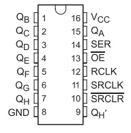
Ping configuration of sn74hc595
sn74hc595 register has 18 pins. which is shown in the image at left. Pin 16 is for VCC, which should be connected to 5v. Pin 8 is connected to common ground in the system. Pin number 1 to 7 and 15 is parallel data output pins. Pin 14 is the serial data input pin. Pin 11 is serial clock pin. when pin 11(SRCLK) goes from Low to High the value of pin 14(SER) is stored into the shift register and the existing values of the register are shifted to make room for the new bit. Pin 12 (RCLK) is used for latch. This pin should be low when data is written in the sift register. When it goes High the values of the shift register are latched to the storage register which are then outputted to pins Q0-Q7. Pin 13 is to enable output. All latch output is enable if this pin is set to low. Pin 10 is use for clear the output state on pins. Output pins will be cleared if low to high pulse is given to this pin. Default value of pin 10 is high.
How to co
So to drive this register, we need to control 5 pins. Pin # 14,13,12,11 and 10. We need to connect output pins to LEDs to check output of shift register. Based on this, we have derived a circuit diagram.
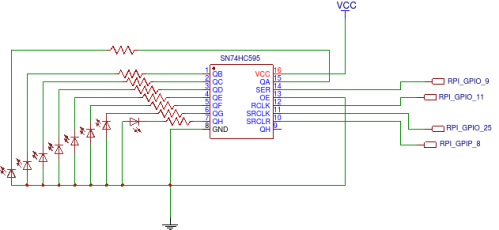
Circuit diagram
Above image shows circuit diagram. Here we are using GPIOs of raspberry pi to control shift registers. RPI GPIO 9 is used as serial data line when is connected to SER(pin 14) of sn74hc595 . RPI GPIO 11 is used as latch clock line which is connected to RCLK (pin 12) of sn74hc595. RPI GPIO 25 is used as serial clock line which is connected to SRCLK (pin 11) of sn74hc595. RPI GPIO 8 is used as serial clear line which is connected to SRCLR(pin 10) of sn74hc595. In addition to this, it is essential to connect VCC ad 5v and Common Ground with RPI.
Now, its time to design driver to control these GPIO pins. Driver will expose sysfs interface to change value represented by leds. Value which is written to this sysfs file will be represented by leds which is connected with sn74hc595.
So, lets start understanding responsibilities of init function of driver. As part of initialization of this driver, we need to Configure pin 21, 22,23 and 24 as GPIO which corresponds to GPIO 8, 9, 25 and 11. In addition to this, we have to resigter sysfs class and device to control shift register.
Les take a deep dive into source code of driver. As first part we have declared to global GPIOs pins which can be used in all driver code. As per our circuit design above we have declared the pins which is shown in below code snippet.
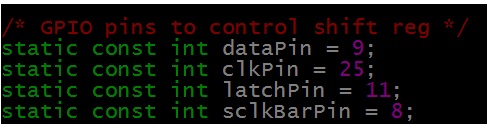
GPIO Declaration
As part of initialization we have to configured this pins as GPIO pins. Below code snippet configures and request this pings as GPIO. The below snippet is part of init function of driver.
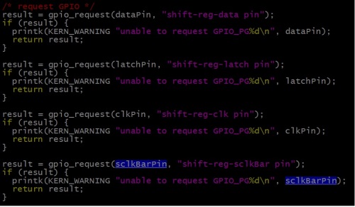
Configure Pings as GPIO
Now we have to configure this pins as output pins and set to appropriate default value. As explained above we need to configure Pin 10(serial clock bar) to high. The default value of all other pins will be low. The below snippet shows this.
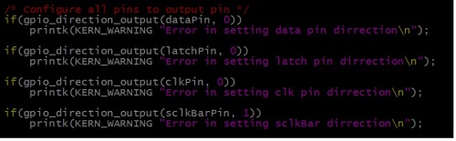
Configure GPIOs as output
Lets register sysfs interface to control output of shift register. I have created new sysfs class and device to represent shift resister.
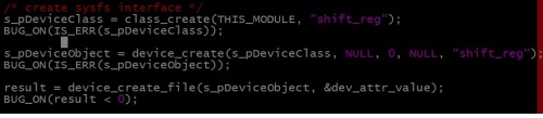
Registration of Sysfs interface
Every device interface in sysfs has attributes which can be read or write. Corresponding read write function registered with the attribute will get called when read or write operation performed on the this interface. Below snippet shows the registration of attribute named value with set and get value callback.
The attribute name should be the same as given by the time of creating file. Here we have given name as dev_attr_value. So out attribute is the value for which we have registered set and get routine. when we tried to read the file(sysfs Interface) from application, get_value_callback will be triggeres in the driver. In case we tried to write some value to file(sysfs Interface) from application, set_value_callback will be triggers with the value to write in shift register.

Registration of sysfs device attribute
On low to high transmission of clock pulse, internal register(storage register) value will shift by one and value on data pin will be moved to LSB of internal register. At the end after 8 bit data is shifted to the shift register, by providing the latch pulse from low to high, all data from the internal register(storage Register) is latched to shift register pins. We have connected LEDs to the output pins of shift register. This is shown by below snippet. To write some value to shift register, it is essentials to put that value on data pin of shift register and then provide a clock pulse. On this clock pulse, data on internal register gets shifted and adds new bit(which is present on data pin) at the end presently shifted data. So here in code, I am setting bit by bit this new_value variable on data pin and after setting one bit providing clock pulse. At the end i am providing the latch pulse so the 8 bit value which stored in the internal storage register will be latched to the pins.
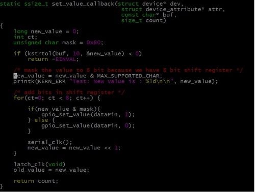
Routine to set value
When user application tries to read the value from the sysfs interface, the get_value_callback will get called. The callback will return old_value which was updated by the get value callback. The below snippet shows that. 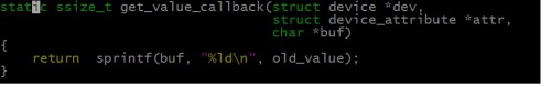
Here you can get full code for this driver. you can follow this steps to add module to Linux kernel source code and compile it.
Cheers !!!


